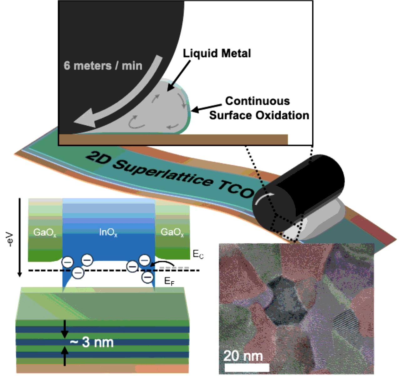
We process these 2D oxides from a rapid liquid metal printing approach that utilizes the solid oxide skin spontaneously rapidly formed via Cabrera Mott oxidation[21]. We have advanced the liquid metal synthesis by developing a novel continuous liquid metal printing (CLMP) method that transforms droplet wise ‘touch printing’ into a high-speed process suitable for R2R deposition of films of highly continuous nanosheets deposited over 10-100 cm2 areas. As depicted in the schematic in Figure 1a, our CLMP method utilizes a compliant rubber roller (Figure S1) to uniformly press a liquid metal meniscus at 1 – 20 cm s-1 at a line pressure of approximately 6 N cm-1. This continuous rolling process transfers the 2D surface oxide to a target substrate such as glass, silicon, or plastic (Figure 1b) where it is held in place by van der Waals force. We have iterated this rapid process to generate multilayer superlattices consisting of periodically alternating layers of InOx and GaOx. For our superlattice structure, GaOx is chosen because it is expected to form a type-I heterointerface known to induce electron donation into InOx. GaOx is also chosen because it is suitable for high-speed liquid metal induced deposition because of metallic Ga’s low melting temperature (Tm = 37 ˚C). Multilayers can be deposited via multiple printing steps to build up thicker films (Figure 1c), requiring only a 2 s atmospheric pressure air plasma treatment in between each cycle to ensure uniform adhesion of the subsequent layers. Figure 1c also illustrates the exceptional uniformity of the CLMP process, which can deposit pinhole free layers across a 150 mm substrate in less than 3 s, without requiring any post-annealing processes. Figure 1d shows a large area scanning microscope image of a single film patterned by CLMP with multiple overlapping InOx and GaOx layers, indicating the high macroscopic areal uniformity that can be achieved.
2.1 Crystallinity of TCO Superlattices
Superlattice films comprising two layers of InOx capped with one layer of GaOx were characterized by HRTEM, as shown in Figure 1e. The 2D films exhibit large InOx crystallites with lateral dimensions from 10 – 30 nm despite their thickness of just 3.5 nm per layer. The HRTEM images of these multilayer films also exhibit Moiré fringes, as highlighted in Figure 1e, an interesting feature characteristic of these 2D oxides that indicates the overlay of crystallites during the CLMP process. HRTEM analysis also shows amorphous regions (GaOx) overlapping the InOx crystallites. An analysis of the grain size from a range of HRTEM images of the superlattice films (Figure 1f) shows an average grain size of approximately 20.0 nm ± 4.7nm. This platelike grain morphology is expected to aid intergrain and interlayer transport, enhancing conductivity. We note that the grain size observed by HRTEM in these CLMP films is substantially larger than that exhibited by ultrathin sputtered In2O3[22] or high quality sol-gel In2O3[23].
Selective area diffraction analysis from the HRTEM images (Figure 2a) shows peaks that can be indexed to the cubic phase of In2O3, with the strongest peak being the typical (222) orientation of InOx. X-ray diffraction (XRD) characterization confirms that 2D InOx films formed by CLMP are crystalline in their as deposited state but the GaOx films printed by this method have been observed to be amorphous across the entire range of deposition temperatures. Figure 2b,c illustrate the XRD spectra for InOx / GaOx superlattice films as a function of deposition temperature from 180 ˚C to 240 ˚C. The superlattice films exhibit the characteristic (222) and (400) peaks of cubic InOx, as do the pure InOx films (Figure 2d). At temperatures from 80 ˚C to 240 ˚C, only the amorphous phase of GaOx was observed for these films. The intensity of the (222) and (400) peaks grows monotonically at higher deposition temperatures, which agrees with our past observations of increases in crystallinity with post-annealing of liquid metal printed InOx films formed at 165 ˚C[24].
Figure 2e also illustrates an interesting trend in the grain size extracted from the (222) XRD peak by the Scherrer Debye equation[25], which decreases from approximately 7.2 nm in the case of the superlattice films printed at low temperatures (180 ˚C) to approximately 5.2 nm for films printed at 240 ˚C. The decrease in the average grain size with increasing deposition temperature runs counter to the trend typically observed for vacuum deposited films, for which higher deposition temperatures provide additional thermal energy for grain growth. This trend could be a result of the nucleation and growth kinetics of Cabrera-Mott surface oxidation.
The texture of these films, as indicated by the relative intensities of the (400) and (222) peaks (Figure 2f), shows preferential orientation along the (222) direction, which is often observed from cubic In2O3. The texture of films is influenced by the deposition temperature and the layer configuration, with higher deposition temperatures favoring grain growth along the (222) orientation—similar to sputtered InOx films[26]. It has also been reported that oxygen content and slower growth can preference the (222) grain growth for sputtered InOx films[27]. This corresponds well with our observations that higher deposition temperatures leading to more rapid Cabrera Mott surface oxidation and more stoichiometric In2O3 formation may also lead to preference for the crystallization along the (222) plane. The most conductive films fabricated in this study have more greater contributions from the (400) orientation, which is similar to the texture reported for highly conductive sputtered In2O3[28].
2.2 XPS Characterization of TCO Superlattices
XPS studies reveal details about the composition and electronic structure of 2D InOx and GaOx in the superlattice structures, showing the changes induced by modulation doping. Figure 3a shows the XPS In 3d3/2 and In 3d5/2 core level spectra for both pure InOx films and modulation doped InOx capped by 2D GaOx. The positions for the In 3d peaks of pure InOx closely match those of recent reports of liquid metal printed InOx films[29]. Interestingly, however, both the In 3d3/2 and In 3d5/2 peaks shift 0.33 eV higher in binding energy after adding the GaOx modulation doping layer. This shift in the In 3d peaks is consistent with the shift reported for modulation doping observed by XPS in tin oxide films[30]. We note that the increase in binding energy is also similar to the shift induced by degenerate extrinsic doping of Sn in 2D ITO[7].
To understand the origins of the modulation doping of InOx provided by GaOx, we consider its oxygen stoichiometry as determined from XPS analysis. Figure 3b shows the O1s spectra for the printed 2D GaOx, InOx, and InOx / GaOx heterostructures. These spectra are decomposed into sub peaks (Table 1) corresponding to stoichiometric M-O bonding (530 eV), oxygen deficient M-O bonding (531 eV), and metal hydroxide M-OH bonding (532 eV). CLMP InOx is dominated by stoichiometric M-O bonding and an oxygen deficient M-O bonding, with a minor contribution from surface hydroxide states. The modulation doped sample’s O1s signal is expected to include contributions from the underlying InOx as well as the 3.5 nm GaOx capping layer, showing the increase in the high binding energy oxygen deficient peak relative to pure InOx films. The high percentage of oxygen deficient bonding in the pure GaOx associated with oxygen vacancies is consistent with other reports of low-temperature liquid metal printed GaOx films[31]. Based on our measurements of the conductivity of superlattices formed with GaOx deposited at lower temperatures (down to 40 ˚C), we expect that the defective, substoichiometric chemistry of CLMP GaOx enhances its effectiveness for modulation doping 2D oxide layers.
Table 1
O1s XPS peak decomposition of InOx, GaOx, and InOx / GaOx films (~ 12 nm thick).
|
Stoichiometric M-O [%]
|
O-Deficient M-O [%]
|
Hydroxide
M-OH [%]
|
|
InOx
|
66
|
19
|
15
|
|
GaOx
|
56
|
27
|
16
|
|
InOx / GaOx Heterostructure
|
67
|
23
|
13
|
2.3 Optical Transparency of TCO Superlattices
An essential benefit of implementing defect modulation doping is the ability to improve optical transmittance through control of the Burstein Moss shift in these 2D TCOs. UV absorption spectroscopy measurements of 14 nm InOx films with and without 3 nm capping layers of GaOx (Figure 3c) reveal that adding the GaOx leads to a reduction in absorption and a blue shift in the optical bandgap by approximately 80 meV, as determined from a Tauc plot extraction of the direct bandgap transition. This blue shift is consistent with the role of GaOx as a modulation doping layer, which induces a higher free electron concentration in the InOx layers. This is an interesting result that runs counter to the conventional assumption that adding additional layers should increase the optical absorption. As Figure S2 illustrates, the modulation doping has the effect of significantly increasing the optical transmittance in the visible range to above 99%, essential for boosting the figure of merit of 2D TCO films for various optoelectronic device applications.
2.4 Electronic Transport in TCO Superlattices
The CLMP 2D oxides demostrate exceptionally high conductivity in their as deposited state considering the rapid total processing time (less than 2 s) and low process temperatures. Similar to any vacuum processed oxide films, the conductivity of these materials depends critically on the oxygen stoichiometry, which varies with the deposition temperature. Conductivity is optimal in the range of 180 ˚C – 200 ˚C for the modulation doped layers as well as pure InOx. The most conductive pure InOx films reach a conductivity of approximately 60 S cm-1 in the range of 180 ˚C – 200 ˚C. In comparison, the most conductive modulation doped superlattice TCOs reach above 600 S cm-1 at a deposition temperature of 180 ˚C, a mark that is on par with the conductivity of sputtered films. We know from the XRD studies that the crystallinity is greater when deposited at higher temperatures (220 ˚C – 240 ˚C). Based on XPS studies, these high temperature deposited films are also expected to be more stoichiometric with fewer oxygen vacancies, matching the trend of substantially lower conductivity for these films. Interestingly, modulation doped films, as shown in Figure 4a, exhibit substantially greater conductivity for higher deposition temperatures because the modulation doping mechanism can overcome the reduction in intrinsic vacancy concentration.
Figure 4b shows the conductivity as a function of the ratio of InOx layers to GaOx layers. Enhancement with modulation doping is more effective for larger ratios of InOx – GaOx. Reaching an optimal value at a ratio of 4-1. This can be understood by considering that GaOx is, itself, substantially less conductive than InOx, with a conductivity of approximately 0.01 S cm-1 (Figure S3), which could limit interlayer transport across the vertically overlapping grains. Our past studies of electronic transport in 2D InOx have shown that this overlap can produce higher electron mobility[24]. To further understand the mechanism of the modulation doping, we also utilized the CLMP to fabricate films capped by CLMP AlOx, SbOx, and SnOx for comparison (Figure 5a) with the conductivity of pure InOx and films capped by GaOx. AlOx shows a significant enhancement in conductivity comparable to GaOx, but SbOx and SnOx have a substantially lower enhancement. This can be understood by considering the equilibrium band diagrams of these materials (Figure 5b). Liquid metal printed SnOx (p-type) and SbOx have lower lying EF‘s that do not facilitate electron donation to the InOx, whereas AlOx and GaOx have shallower donor defects that can facilitate modulation doping. We note that modulation doping is also particularly successful in inducing high carrier concentration in these combinations of 2D InOx and wide bandgap GaOx because of the low processing temperatures available for both layers. The low process temperatures are essential in order to avoid compensation by acceptor type defects[30] that otherwise nullify gains in the free carrier concentration.
Room temperature Hall measurements (Figure 6a) of the TCO superlattice films show the influence of modulation doping for enhancing both the carrier concentration as well as the Hall mobility (μ0). Films printed at 180 ˚C and 200 ˚C both exhibit the modulation doping effect (Figure 6b) of the GaOx heterointerface, which increasse the carrier concentration by more than 10X to above 1020 cm-3, consistent with our observations of the Burstein Moss shift in the optical bandgap. The Hall mobility of the undoped InOx films are 6 cm2V-1s-1 and 33 cm2V-1s-1 at while modulation doped films are enhanced to nearly 40 cm2V-1s-1 even with the large increase in carrier concentration. For films processed at just 180 ˚C without any vacuum processing, the observed Hall mobility is exceptional compared with solution-processed materials based on sol-gels or nanoparticles[32], indicating the extremely high electronic quality of CLMP 2D oxides. This result is also consistent with our recent report of liquid metal printed 2D InOx transistors with field effect mobility as high as 67 cm2V-1s-1[24]. The films with the highest carrier concentration in the range of 8 · 1019 – 2 · 1020 have slightly lower Hall mobility in the range of 10-15 cm2V-1s-1, which may indicate that these heterostructures induce additional trapped carrier scattering[33]. Collectively, our results are consistent with recent reports of defect modulation doping in amorphous and polycrystalline sputtered films. For example, Weidner et al. report defect modulation doping of SnO2 with AlOx[30] producing a 10X increase in both carrier concentration and mobility for modulation doped SnO2. In this case, the authors relate the increase in μ to the decrease in the ground boundary energetic barrier height, which is one potential explanation for the enhancement to mobility in our polycrystalline InOx films.
The CLMP 2D oxides developed here exhibit lower process temperatures but higher conductivity than printed TCOs formed by methods such as gravure and inkjet. The advantage of our method is also that it can deposit highly crystalline but ultrathin 2D oxide layers – we have observed that the liquid metal printing method allows crystallization at much lower temperatures than sol-gel materials[24]. One advantage of these low temperature processing methods is facilitating device applications in structures such as photodetectors or printed thin film transistors[34], which can benefit from the high conductivity and high transmittance of 2D oxides.
The enhanced conductivity of these films is presented in comparison to recent literature reports of printed TCOs based on sol-gels and nanoparticles in Figure 6c[7], [35–50]. A primary aim in this field is to produce highly conductive TCOs using a minimal thermal budget to allow use of low-cost flexible polymer substrates, which have a thermal limit around 200 ˚C. Improving the conductivity of these films could directly translate to an increase in the performance of large area printed electronic device such as electrochromic windows, thin film solar cells, and thin film transistors. As shown in Figure 6c, CLMP 2D oxides offer a combination of both these critical properties that has not been attained via nanoparticle or sol-gel printing techniques. This trend is observed because nanoparticle films are strongly limited by interparticle transport, requiring high temperatures to sinter the particles and improve conductivity. Similarly, sol-gels suffer from low conductivity due to insulating residues from incomplete decomposition of metal salt precursors at low-temperatures. We also stress an essential benefit of our CLMP method, which is that the integrated thermal budget is exponentially smaller due to the elimination of long (~ 1 hour) post-annealing steps used in most printed TCO processes. This rapid low-temperature processing and high conductivity make our novel CLMP approach an ideal candidate for upscaling printed inorganic electronics.