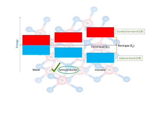
The intrinsic optical and electronic properties of semiconductor material play an important role in constructing an efficient solar cell. The critical property of a solar cell depends on whether the semiconductor absorbs the wide range of photons that are contained in solar radiation. The magnitude of such absorption deals with the active layer of an absorber, the wavelength of radiation, and the absorption coefficient. These parameters are directly related to the semiconductor’s band gap energy (Eg) and band structure energy (Eb). Photons with higher energy than the absorber’s Eg can be absorbed and can generate an electron-hole pair. The excess energy is converted into heat in the solar cell. Using a wide range of wavelengths results in low photocurrent of a solar cell with high efficiency and probability, because, that high fraction of photons is being converted into electricity and voltage. On the other hand, solar cells are usually made of semiconductors with narrow band gaps which can absorb a smaller region of radiation but higher energy photons that leads to a lower photocurrent and voltage. Therefore, to achieve the maximum conversion of energy and efficiency, an absorber should have the optimum Eg [1]. The other important concept is the band structure (BS) which can explain the optical and magnetic properties of a crystal. The level of Fermi energy (EF) determines the nature of the material. If the EF is located in a band gap zone, the material is considered as insulating (or semiconducting) otherwise it is metallic [2]. In an insulator, the highest occupied band is called the valence band (VB) and the lowest unoccupied band is known as the conduction band (CB), at zero temperature (Fig. 1).
On the other extreme, in a conductor, the CB is occupied with electrons, even at zero temperature [3]. By applying an electrical field, electrons can easily jump across the band gap toward the CB, at any temperature above zero. The high energy of electrons can be obtained from thermal motion or agitation. The Eg of an insulator usually is 5 eV or above which means the required energy for jumping electrons is less available which leads to a weak electric current or lack of it in presence of an external electric field. Most of the important semiconductors show the Eg values range between 0.25 to 2.5 eV [4–6]. Silicons, which are widely used in electronics, solar cells, and, biomedical and light-emitting devices, show the indirect band gap nature of the BS. The indirect band gap of silicon has been a chief obstacle until the last two decades. Various effort has been devoted to the study and use of nanoscale Si-based substances to discover and improve their optical properties in the last years. Silicon nanocrystals display the visible photoluminescence that proves the partially overcoming their indirect band gap. Nevertheless, there are still many aspects to discover and dispute [7]. In this investigation, we conduct the BS, density of states (DOS), k-resolved DOS, and spin-orbit coupling (SOC) calculations for the optimized SiC nanocrystal, using the plane-wave (PW) method as implemented in Quantum Espresso (QE) program [8–10], based on the density functional theory (DFT) (Fig. 2).