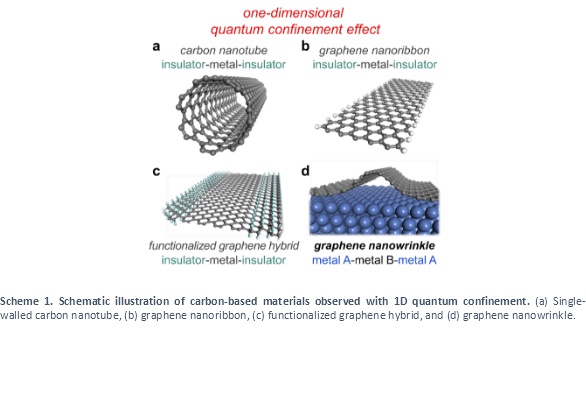
A GNW with a width (w) below 5 nm can be synthesized on an atomically smooth Ni(111) surface under ultrahigh vacuum conditions using an extremely rapid cooling method (Figs. 1a and b). The unique electronic structure of GNWs was revealed through STS (Fig. 1c). The sharp dI/dV peaks around the Fermi level (EF) assigned as vn and cn (n = 1 and 2), which were obtained at the center of the GNW (w = ~ 2.4 nm), indicate the discrete energy levels in the valence and conduction bands of the GNW, respectively. The Landau levels due to the strain-induced pseudo magnetic field24,25 can be excluded as a cause of the formation of discrete energy levels by considering the characteristics, such as peak positions and the width-dependent inversely proportional change in the energy gap. In particular, the lack of the zeroth Landau level in the STS spectrum and the independence between the curvature of the GNW and energy gap were suggested as counterevidence for excluding the possibility of the Landau levels in interpreting the discrete energy levels of GNW. Another possibility for the experimental observation could be the vHS, i.e., the singularity in the DOS of the GNW, owing to 1D electron confinement at the nanoscale. However, the electron confinement of the 1D GNW via the gradual geometric deformation perpendicular to the graphene plane without explicitly destroying the π-conjugated bonding network is an extraordinary electronic behavior, owing to the lack of a large potential barrier crossing the wrinkle (GNW) and flat (epGr) regions of the metallic graphene sheet.
To interpret the physical origin of the unusual electron confinement in GNW resulting in vHS, we systematically conducted periodic DFT calculations for the GNW on Ni(111). The influence of the interfacial interaction with the metal substrate on the electronic structure of GNW was addressed by employing Cu(111) because Cu is known to weakly interact with graphene in contrast to Ni strongly interacting with graphene26. The optimized interfacial distances (d) were 2.24 and 3.27 Å for epGr/Ni(111) and epGr/Cu(111), respectively (Supplementary Fig. 1), which correlated with reported values27,28,29. To specify the GNWs with the simplest directionality, we used the notation of armchair and zigzag GNW (aGNW and zGNW), according to the atomic arrangement along the transverse direction of GNW (Supplementary Fig. 2): Four positive integer values (α, β, i, and j), were used to define the vector along the arc of the GNW (LA) by a linear combination of the graphene unit vectors (α and β) and the vector along the basal line (LB) under the arc of the GNW by a linear combination of the unit vectors of the metal surface (i and j). Therefore, the direction of the GNW and its dimensions (width (w) and height (h)), were defined as (α,β)/(i,j)-GNW/metal: aGNW and zGNW are described with the proposed notations, (k + x, k + x)/(k, k)-GNW/metal (α = β = k + x (x > 0); i = j = k) and (k + x,0)/(k,0)-GNW/metal (α = k + x (x > 0); i = k; β = j = 0), respectively (Supplementary Table 1 and Supplementary Fig. 3), where the w(h) of the GNW increased as k(x) increased.
The electron density redistributions at the interfaces of zGNWs on Ni(111) and Cu(111), (9,0)/(8,0)-GNW/Ni and (9,0)/(8,0)-GNW/Cu, were examined using the charge density difference (Δρ) maps to estimate the interfacial interaction of GNW/metal (Fig. 2; see also Supplementary Fig. 4 for aGNWs on both substrates, for which the interpretation was identical to that for zGNWs). The dimensions (width and height) of the zGNWs were comparable with those of an experimentally synthesized GNW (Fig. 1). The larger charge redistribution observed at the interface of the epGr region of the GNW/Ni model, compared with that of GNW/Cu demonstrated the chemisorptive characteristic between the epGr and Ni(111) as reported (see Supplementary Fig. 5 for the physisorptive characteristic between epGr and Cu(111))29. The considerable hybridization of the pz orbitals of the epGr with the 3d orbitals of Ni(111) may have enhanced the sp3 bonding characteristics in the π-conjugated bonding network of pristine graphene. Consequently, the electron density was substantially localized between the C–Ni bonds instead of the wide distribution throughout the entire graphene layer. Therefore, we suggested that the strong interaction between epGr and the Ni(111) surface was critical for facilitating the formation of the GNW on Ni(111) by overcoming the instability due to the structural deformation and for causing electron confinement along the GNW. Noteworthily, the interfacial C–Ni distance of the carbon atoms at the boundary between the epGr and GNW regions marked with yellow arrows (Fig. 2) was slightly shorter than that of epGr/Ni(111) by ~ 0.1 Å, from which the strong interfacial interaction at the boundary region was expected to contribute to the separation of the electron motions between the epGr and GNW regions.
The electronic band structures of the GNWs on the metal surfaces were investigated to clarify the effect of the relatively stronger hybridization between the epGr and Ni(111), compared with that of the Cu(111) metal surface on the electronic structures. We employed (6,6)-aGNW and (9,0)-zGNW because their dimensions were mostly comparable to each other (Fig. 3): for aGNW, the w and h of (6,6)/(5,5)-GNW/Ni were 21.3 and 6.5 Å, respectively, and for zGNW, the w and h of (9,0)/(8,0)-GNW/Ni were 19.6 and 4.8 Å (see Supplementary Table 1). Considering that many bands originating from the d orbital of the metal substrate were widely distributed near the EF, the projected bands to the C pz orbitals are highlighted as shown in Fig. 3. The red and green-dotted bands corresponded to the pz orbitals of carbon atoms at the GNW and those at the epGr, respectively. The most important finding in the band structures of GNW/Ni was that the pz states of GNW were obviously separated from those of the epGr regardless of the directionality of GNW (Figs. 3a and b for aGNW and zGNW, respectively). In contrast, the positions of the pz states of GNW substantially overlapped with those of the epGr on Cu(111), although their contributions differed depending on the directionality of the GNW (Figs. 3c and d for aGNW and zGNW, respectively). The Dirac-cone electronic structure at the K point of the first Brillouin zone (BZ) is one of the most prominent features in the electronic structure of the graphene layer and was reported to be deformed by strong interfacial electronic coupling with Ni(111), as opposed to that of the graphene interacting with Cu(111)29,30. We also observed the robust band mixing with the C pz orbital of the epGr and Ni d orbital, as expected (Figs. 3a and b). In particular, the C pz states of GNW spatially separated from the epGr exhibited a great degree of the disappearance of the Dirac-cone electronic band structure. However, in the electronic structures for the GNWs on Cu(111), the Dirac-cone structure was well preserved near the EF in the band structure for aGNW and zGNW (Figs. 3c and d). This also implied that the interaction between the epGr and metal substrate was a critical cause for the vHS by breaking the π-conjugated bonding network. It is noteworthy that the Dirac-cone structure of the GNW on the metal substrate was observed at a different wave vector position from the K point in the first BZ of pristine graphene, which can be understood by the band folding, owing to the smaller first BZ for the supercell of the GNW on the metal substrate (Supplementary Fig. 6)31. The 1D confinement behavior of GNW/Ni may also be supported by the reduced distribution of dispersive bands and the enhancement of flat bands (blue arrows in Fig. 3) along the transverse direction across GNW, i.e., Γ–Y and Γ–X for aGNW and zGNW, respectively, in their band structure, relative to those of GNW/Cu. The bandwidth and contribution of the C pz orbital in the dispersive band were more reduced in GNW/Ni, compared with those in GNW/Cu. According to the simple tight-binding method, the bandwidth, i.e., the energy range of the dispersive band, becomes narrower as the overlap energy reduces due to the improved confinement effect. Therefore, we suggested that the flattened dispersive curves prominently appeared in GNW/Ni in the direction across GNW, as a feature reflecting the pseudo 1D electron confinement in the GNW/Ni system. The influence of the arc-shaped GNW geometry on the electronic structures of GNW was elucidated using the band structure of the freestanding GNW without a substrate, which was obtained in a manner of single-point calculation (Supplementary Fig. 7). The negligible change in the electronic band structure of the freestanding GNW, compared with that of the pristine graphene indicated that the interaction between the epGr and Ni(111) can be considered more important than the strain effect for determining the electronic structure of the GNW on Ni(111).
Compared to other 1D nanomaterials, the dimension of the confined length in the pseudo 1D GNW/Ni system was unclear, owing to the ambiguous borderline between the GNW and epGr. Therefore, we attempted to compare the electronic band structures of GNW/Ni and the H-terminated curved GNR (cGNR). The curvature of cGNR was the same as that of the corresponding GNW/Ni model, and its arc length was reduced to unveil the effective confined length (Lec) of GNW by discovering the comparable cGNR structure. As a representative system, the (6,6)-cGNR and (9,0)-cGNR structures were created by removing the atoms of the epGr and Ni substrate from the fully optimized structures of (6,6)/(5,5)-GNW/Ni and (9,0)/(8,0)-GNW/Ni, respectively, and the attached hydrogen atoms were only optimized (Fig. 4a). The reduced arc length is denoted by, e.g., (α-l,β-l)-cGNR, corresponding to (α,β)/(i,j)-GNW/Ni, where l is the number of benzene moieties removed from both edges of (α,β)-cGNR (Supplementary Fig. 8). Although the antiferromagnetic (AFM) state of the armchair GNR (aGNR) was slightly more stable than its ferromagnetic (FM) states (Supplementary Fig. 9), the GNW on Ni(111) exhibited FM characteristics in its spin density map because of the influence from the Ni substrate (Supplementary Fig. 10). The electronic band structures of FM cGNRs were used for appropriate comparison with GNW/Ni. The band structures of (6-l,6-l)-cGNR (l = 0–3) substantially resembled that of (6,6)/(5,5)-GNW/Ni (Figs. 4b and Supplementary Fig. 8). Thus, GNW/Ni was considered to exhibit a similar electronic structure to those of definitely 1D confined cGNRs. Further prudent comparison determined the band structure of (6 − 2,6 − 2)-cGNR as the closest to that of (6,6)/(5,5)-GNW/Ni (Fig. 4c). Therefore, the Lec of the GNW was shorter than the full range of the GNW (L) region on Ni(111). The prominent feature of 1D electronic confinement, i.e., the formation of discrete DOS, was revealed by plotting the C pz-projected local DOS (LDOS) for (6,6)/(5,5)-GNW/Ni and (6 − 2,6 − 2)-cGNR, which can be interpreted as the formation of 1D vHS in GNW and GNR (Fig. 4d). Here, (9 − 3,0)-cGNR was determined as the closest electronic band structure to (9,0)/(8,0)-GNW/Ni (i.e., zGNW/Ni) in the same manner to aGNW/Ni (Figs. 4e–g). The allowed electron wavevectors for aGNWs always crossed the Dirac point of graphene by considering the correlation between the BZ of GNW superimposed with the primitive BZ of graphene (Supplementary Fig. 11). Therefore, the small energy gap between the v1 and c1 (ΔEg) of aGNWs was attributed to the splitting of the Dirac-cone. In contrast, the condition of zGNW (whether the allowed electron wavevector crosses the Dirac point or not) was determined by the size of its Lec. Thus, the types of zGNWs are categorized into three classes of N = 3q, 3q + 1, and 3q + 2, where N is the size of a zGNW unit vector, and q is a positive integer (Supplementary Fig. 12). Therefore, the ΔEg values of zGNWs can be determined from their electronic band structures depending on the class of zGNW.
The correlation between the theoretical value of ΔEg and the arc length of GNW was investigated to explain the experimentally obtained ΔEg values of GNW, which were inversely proportional to the arc length of GNW18 (Fig. 5). The positions of 1D vHSs for (6,6)/(5,5)-GNW/Ni were assigned to v2 = − 0.67 eV, v1 = 0.00 eV, c1 = + 0.16 eV, and c2 = + 0.71 eV (Fig. 5a-i). The positions of 1D vHSs for (7,7)/(5,5)-GNW/Ni and (8,8)/(5,5)-GNW/Ni, with dimensions of large height (h) and same width (w), compared with those of (6,6)/(5,5)-GNW/Ni are shown in Figs. 5a-ii and a-iii, respectively. The positions of 1D vHSs for the zGNWs were investigated by an identical approach (Fig. 5c): (i) (9,0)/(8,0)-GNW/Ni; (ii) (12,0)/(8,0)-GNW/Ni; and (iii) (15,0)/(8,0)-GNW/Ni). It is noteworthy that the zGNWs belonging to the class of N = 3q were only considered for excluding the effect caused by the class difference. The electronic band structures for other classes of zGNWs (N = 3q + 1 or 3q + 2) are provided in Supplementary Fig. 12. As indicated in the schematic electronic structure near the Dirac-cone shape, the allowed electron wavevector (black line) for aGNW (Fig. 5b) and zGNW (N = 3q + 2) crossed the K point, whereas that for and zGNW (N = 3q or 3q + 1) (Fig. 5d) did not cross the K point. The class-dependent K point selection rule for zGNWs is consistent with that for the aGNRs considering the correlation between the classes of zGNWs and aGNRs as explained in Supplementary Fig. 12. The change in ΔEg for aGNW and zGNW (N = 3q + 2) as a function of Lec is plotted in Figs. 5b and d, respectively. They revealed the inversely proportional correlation, which was agreed with the experimental observation well18.
Additional fascinating insights into the 1D confinement of GNW/Ni can be discovered using the band-decomposed charge density (|Ψn|2) analysis because its shape along the confined dimension should reflect the standing waves within the “1D particle-in-a-box model” (Fig. 6). The wave functions (Ψn) with respect to the confined dimension of L were expressed as \({\varPsi }_{n}=\sqrt{\frac{2}{L}}\text{sin}\left(\frac{n\pi x}{L}\right)\) when the potential energy was assumed to be zero inside the 1D box. The index, n, is called the principal quantum number, and x is the coordinate of the particle. The wave functions, Ψn (n = 1–4), in the 1D particle-in-a-box model (Fig. 6a) can be transformed into those in the curved 1D box (Fig. 6b), which corresponded to the cross-sectional shape of the GNW. The probability distribution of the electrons was determined by |Ψn|2, and the n − 1 node should have been observed in |Ψn|2. We explored the band-decomposed charge density distributions and corresponding wavefunctions for the electronic states at the Γ point from − 4 to + 3 eV of (9,0)/(8,0)-GNW/Ni. Among the states that the C pz orbitals mainly contribute, the quantized standing waves described by “1D particle-in-a-box model” were confirmed as displayed in Fig. 6c. Ψ1 was observed at the lowest level at − 2.32 eV in the valence band with zero number of nodes. Ψ2, Ψ3, and Ψ4 were observed at − 1.98, − 1.66, and − 1.52 eV with n − 1 nodes in the order of increasing energy level, respectively. These significant findings are suggested as the strong theoretical evidences of the 1D electron confinement in the GNWs grown on Ni(111).