The prepared plastic sample, as shown in Fig. 2a, was put into the electrolyte A, the spiral coil after electrodeposition is shown in Fig. 2b. Using an impedance analyzer to measure the inductance and impedance of spiral coils. And the magnetic field generated by the solenoid was measured with a gauss meter at different current intensities.
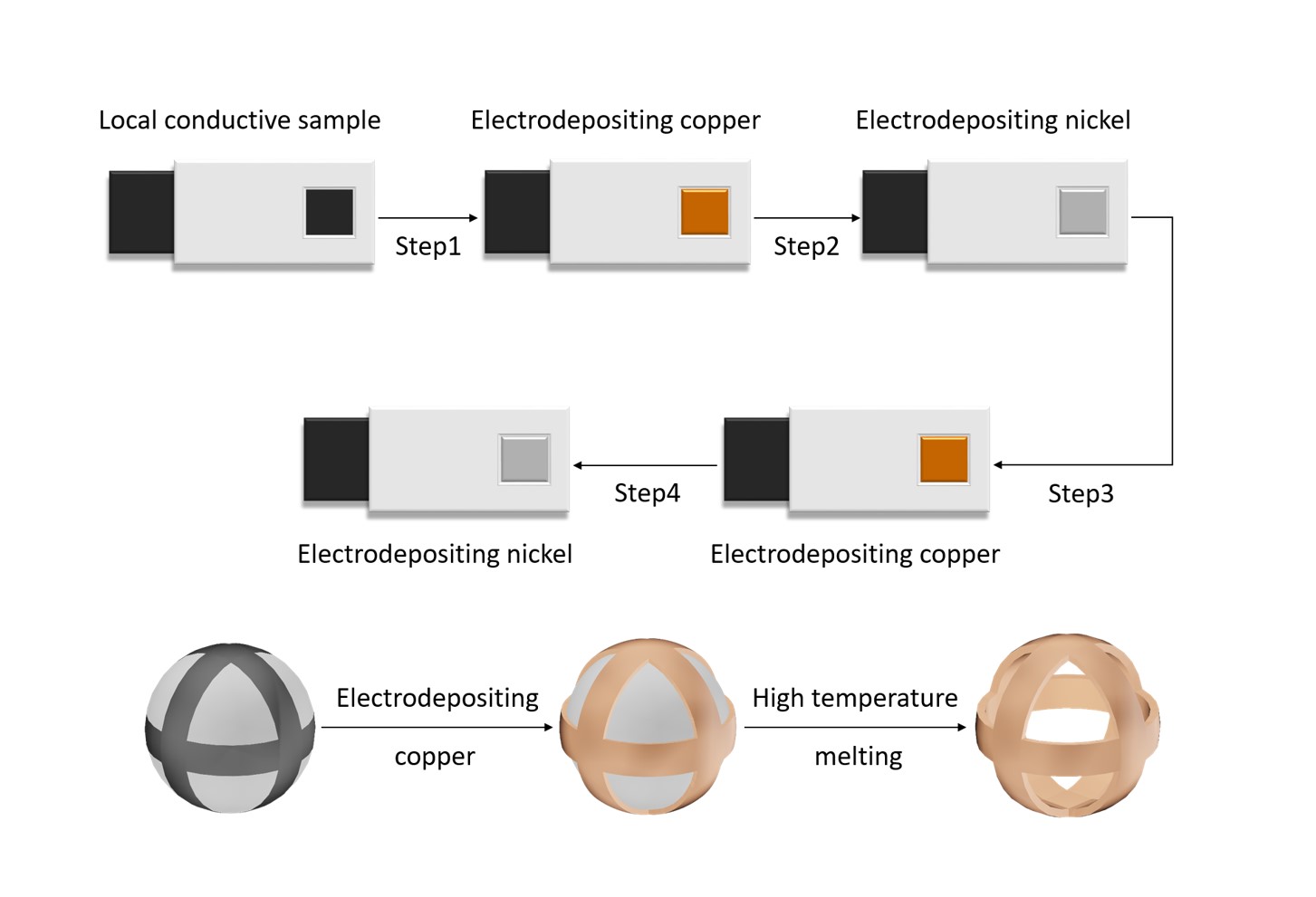
Then prepared a plastic interdigitated battery sample as shown in Fig. 2c. Connect the end of A to anode of the power supply, and the phosphor copper plate to cathode. Subsequently, the sample was electrodeposited in 200 ml electrolyte (20 g CuSO4·5H2O, 10 ml H2SO4 and 40 mg PEG) for 6h at 30mA, washed in distilled water to remove residual electrolyte. Afterward, connect the end of B in the sample to the anode of the power, and cathode to zinc. Electrodeposited the sample in 200 mL electrolyte (60 g ZnSO4·7H2O, 6 g H3BO3) for 6 h at 30 mA. After cleaning, the sample as shown in Fig. 2d was obtained.
After the A and B ends of the sample are connected to the wire and the voltmeter (range 1 V), the sample is placed in 10 vol% sulfuric acid, and the deflection of the voltmeter is observed. When putting the sample into sulfuric acid, the pointer of voltmeter is deflected, and stable at about 0.4 V as shown in Fig. 2e. Zinc on the sample reacts with the sulfuric acid, so the plastic substrate is exposed, the electrons lost by zinc atoms flow to copper through wire, zinc atoms are oxidized to zinc ions, meanwhile hydrogen escapes from the copper surface, hydrogen ions get electrons and reduce to hydrogen, and electrons are transferred from B to A, thus the current is from A to B. The prepared copper-zinc battery can generate a voltage of 0.4 V, demonstrating the outstanding ability of energy storage elements with excellent electrical communication, and computer technology. The selective electrochemical deposition additive manufacturing is simple in operation, low in cost, and saves complex installations and molds, and has huge advantages in micro-scale electronic components. Local conductive plastic samples after depositing copper in electrolyte (100 g/L CuSO4•5H2O) were shown in Fig. 3a, in which copper was well deposited in the conductive area of square, cross and strip samples respectively.
Moreover, the deposition is uniform and even micron scale electronic circuits play a crucial role in network without obvious defects, fully proving the feasibility of selective electrochemical deposition of metal on the local conductive substrate.
As shown in Fig. 3b, the copper sheets all hold intact square shape and uniform deposition overall. Afterwards, the micro morphology of the upper surface on metal sheet was observed by scanning electron microscope as shown in Fig. 4(a, b, c, e, f). With the gradual increase of deposition time from 2, 4, 6, 8 to 10 h, the grain size of copper rises, corresponding to the aggravated surface roughness. Among them, the metal sheet for 2 h shows the smoothest surface morphology without uneven bulge and particle defects, and exhibits uniform grain size in the SEM image of its upper surface.
According to Fig. 3c, with the deposition time lengthening, the mass of the samples gradually rises in linear relation, indicating the current efficiency remains in a relatively stable state during the increasing deposition time. It demonstrates, as the deposition time increases, preparing the metal parts by the selective electrochemical deposition can achieve the relatively stable current efficiency and obtain the roughly steady quality of the metal per unit.
The complex 3D metal components, helical line and hollow sphere prepared are shown in Fig. 5a and 5b. The resulting black material on the surface of the 3D metal parts corresponds to carbonized PLA and residual CNTs.
When heating the bimetal sheet sample by alcohol lamp, with the extended time, the sample gradually bent to the side of nickel, and the deflection angle increased likewise. When returning to room temperature, the sample generally returned to the original shape, as shown in Fig. 5c.
Owing to the greater linear expansion coefficient of copper than nickel, when heated equally, the thermal deformation length of copper is greater than nickel, hence the sample will deflect to the side of the nickel. When returned to room temperature, the thermal expansion part of copper and nickel will shrink, namely, the sample will roughly return to its original shape.
When a layer of copper with identical thickness is deposited on the other side of nickel, the thermal deformation of copper on both sides will cancel when heated, and the sample will not be bent in this area, so the sample can be programmed and designed. According to the design intent, the specific area of sample can be processed into a three-layer structure of copper-nickel-copper or nickel-copper-nickel, while the other parts have a double-layer structure of copper-nickel, as shown in the Fig. 5d. During heating the sample, a specific area will bend, while other areas will remain in their original state. It is also possible to adjust the distribution direction of copper and nickel in each double-layer metal area to regulate the bending direction of the sample.
As shown in Fig. 5(e, f, g, h), there appeared defects in the four deposition areas of sample e) that no metal was deposited at 30 mA, indicating too less copper was produced to fully cover the deposition areas. Whereas the deposition in two areas on the left of sample f) was uniform without defects at 40 mA, there existed more obvious defects in two areas on the right. Further increasing the current to 50 mA, there showed only a few defects in the upper right area of the sample g), demonstrating the further increased quality of deposition. When tuning to 60 mA, no defects occurred in sample h), exhibiting the highest deposition quality and complete coverage in the equal deposition areas. In addition, the grain size of deposited copper remains uniform roughly under the four current intensities, illustrating the increased current intensity did not obviously change the morphology of metal layer, and can also enhance the deposition quality through elevating current intensity. Therefore, if the array structure sample has enough deposition area and appropriate current intensity, it can simply realize the large-scale production of metal electrochemical additive manufacturing.
The edge section of bimetal sheet 1 and four-layer metal sheet 2 was ground with sandpaper, then observed the cross-sectional morphology by metallurgical microscope. Through Fig. 6a and Fig. 6c, the copper layer and nickel layer were well combined with no gaps between layers. Subsequently, cut the sheet 1 and sheet 2 in the middle, and observe the cross-section of the middle part of the sheets. In view of Fig. 6b and Fig. 6d, the thickness of middle is slightly smaller than edge, the copper layer and nickel layer combine tightly in the middle with no cracks.
The intrinsic color of the sample cannot be directly observed under the scanning electron microscope, that is, the copper-nickel binding interface of the sheet cannot be observed, only the fracture morphology of sheets 1 and 2 is legible, and the thickness of each layer was roughly measured. Figure 6e shows the upper metal of sheet 1 is nickel with a thickness of about 112.0 µm and the lower metal is copper with a thickness of about 98.54 µm. In addition, the morphology of the fracture surface of sheet 2 is shown in Fig. 6f, wherein layers are nickel, copper, nickel, and copper from top to bottom, and the thickness is 79.91, 88.09, 50.78, and 76.67 µm separately. In addition, the bimetallic strip has a compact metal structure and its layers are closely bonded, which fully proves the superiority of this method in preparing multi-metal parts.