The chemical structures of diammonium iodide molecule (DIM) with aryl and alkyl chains used as a bonding-regulated molecular passivator are depicted in Fig. 1a. These molecules in isopropanol were introduced on the 3D-HP film as an interfacial passivation layer (IPL) as shown in schematics (Fig. 1b, c). The surface morphology of MA/Br-free HP film (treated without and with PEDAI or PZDI) was studied with scanning electron microscope (SEM) measurement (Fig. 1d-f). One can notice a slight change in the grain size with an overlayer surface grown on the film. The HP film with PEDAI passivation grows with unevenly distributed small crystallite. It suggests that the DIM with an alkyl core has beneficial surface coverage compared to the aryl core. The film with PZDI treatment forms well-covered surface and grain boundaries which is propitious for the elimination of localized defects in perovskite film.7,11
We collected X-ray diffraction (XRD) results of control and surface-treated perovskite films to study the crystal growth. (Fig. 1g, S1a,b) shows XRD of the PEDAI or PZDI-treated HP films with reference to the control film. The PZDI-treated HP films show a dominant (110) characteristic diffraction peak of the α-phase of FA- HP. It suppresses the δ-Cs/RbPbI3 phase and residual PbI2. Moreover, additional peaks at 2θ < 10o are dominantly grown on the HP films with a higher content of DIM indicating the evolution of a 2D phase of PEDAI and PZDI interacting with PbI2.31 The characteristic XRD peak at lower 2θ on the HP film with PEDAI treatment grows with higher intensity indication higher tendency for the formation of 2D phase compared to alkyl counterpart.
Figure 1h depicts the absorption spectra of the control and DIM-treated HP films (varying concentration; Fig. S1c, d). No significant difference was seen at the band edge of the HP film (insets in Fig. 1h, Fig. 1a, c). The PL spectra (Fig. 1i) of HP with PZDI demonstrated an intensified peak while PEDAI suppressed it. The varying PL intensity of HP films treated with different concentrations of DIM (Fig. S2) correlates with improvement in opto-physical quality. One can see a negligible shifting of PL characteristics peak (~ 817–818 nm) suggesting no incorporation of these additives in the 3D-HP lattice. It is also consistent with XRD patterns.
To get more insight into the 2D-phase formation, we prepared HP film by mixing DIM in perovskite precursor solution as depicted in supporting information (Figure S3a1, b1). XRD patterns (Figure S3a2, b2) demonstrated a more intensified XRD peak at 2θ < 10o for the HP film prepared with mixed DIM compared to that with surface treatment. Importantly, the HP film with mixed PEDAI was found to be grown with much higher XRD peak intensity at ~ 4.8o indicating more preference for 2D phase formation. SEM images (Figure S3a3, b3) display nano-sheet-like features in the HP mixed with PEDAI implicates PEDAI-based 2D phase. This is consistent with the small crystallite observed in PEDAI passivated film. Interestingly, unlike PEDAI mixed case, the HP film with mixed PZDI grows with overlayer on crystal grain or at grain boundaries rather than flake structure which is in line with the passivated film. The PL spectra of respective HP films (Figure S3c) also showed characteristic PL peaks at higher energy regimes suggesting the existence of DIM-based 2D phases. The PL characteristic features of respective films are parallel to XRD patterns. These results suggest the HP film with PEDAI can preferably form 2D phases rather than forming a well-covered 3D-HP surface. It is believed that these characteristics differences could dominantly affect the device performance.
To investigate the effect of surface treatment using DIM with aryl or alkyl core on the photovoltaic properties, we fabricated HPSCs with inverted device configuration as depicted in Fig. 2a. A typical cross-sectional image of a complete device is displayed in Fig. 2b. The current density-voltage (J-V) curves for the best HPSCs without and with PEDAI or PZDI treatment are shown in Fig. 2c with a large device area of ≈ 1 cm2. The J-V characteristics with varying concentrations of DIM are given in the supporting information (Figure S4). The device parameters have been summarized in Table 1(Table S1, S2, Supporting Information). The HPSCs with PZDI-treated HP (1 mg/ml) demonstrated champion PCE of ~ 23.17% with negligible J-V hysteresis. However, unlike our expectation, the PCE of the PEDAI passivated device rolls off with reduced JSC and FF with reference to the control device as given in Table 1. A decrease of Jsc and an increase of Voc (both small) seem to be typical behavior of slight passivation of interface defects. It suggests that PEDAI has an interface passivation effect to some extent. These results corroborate that the amine in DIM with aryl and alkyl core greatly affects the device results. It is a consequence of the chemical interaction of the HP with DIM that drives the film quality impacting morphology, surface chemistry, and defect profile. It is known that PEDAI has delocalized lone pair of electrons of nitrogen atoms while that in PZDI is localized. The nitrogen site in DIM enhances the surface adhesion on the HP film which is favorable for defect mitigation. This could result in a stark characteristic difference in HPSCs. We will discuss more insight in the succeeding paragraph accounting for these aspects.
We validated HPSCs with MA/Br-free HP film with PZDI treatment of PCE ≈ 21.47% (area ≈ 1.024 cm2) under standard conditions (accredited independent photovoltaic test laboratory, AIST PV Lab, Japan). The official certified data is given in Figure S8 (Supporting Information). Our certified PCE of the champion device has a record-level device efficiency for inverted p-i-n configuration of HPSCs with MA/Br-free HP for a large area of > 1 cm2. For comparative evaluation, the few certified device reports with an area > 1 cm2 are tabulated (Table S3, Supporting Information), where the champion HPSC compares favorably amongst the reports.
Table 1
Solar cell data and VOC deficit of the HPSCs with MA/Br-free perovskite (without and with surface treatment (PEDAI or PZDI)). \({E}_{g}^{a}\) calculated from EQE data.
| Condition | \({E}_{g}^{a}\) (eV) | | JSC (mAcm− 2) | VOC (V) | FF | PCE (%) | VOC deficit (\({E}_{g}^{a}\)/q -VOC) (V) |
|---|
| Control | 1.513 | F | 23.62 | 1.104 | 0.717 | 18.69 | 0.402 |
| R | 23.56 | 1.112 | 0.750 | 19.65 |
| PEDAI | 1.517 | F | 22.98 | 1.142 | 0.703 | 18.46 | 0.381 |
| R | 22.79 | 1.145 | 0.736 | 19.21 |
| PZDI | 1.515 | F | 24.76 | 1.185 | 0.772 | 22.65 | 0.327 |
| R | 24.78 | 1.188 | 0.787 | 23.17 |
Figure 2d presents the PCE statistics of the control device and with PEDAI or PZDI treatments (Figure S5,6,7 and Table 1,2; Supporting Information). These results indicate better device reproducibility with respective DIM passivation with varying concentrations. For PZDI, the device performance is found to be improved with an increase in all device parameters. However, the device with a higher concentration of PZDI rolls off with a lower VOC and FF. Although the HPSCs with PEDAI treatment are inferior to the control device, the device with a higher concentration of PEDAI further deteriorates by dropping VOC and FF as like the PZDI case. This identical trend could be due to the accumulation of 2D HP phase on the surface unevenly. This observation is in line with other reports.18,31
The external quantum efficiency (EQE) data for HPSCs without and with DIM passivation are shown in Fig. 2e. The EQE response for the device with PZDAI presents a better spectral response in the absorption energy band range of the HP layer (λ > 450 nm) and interfacial regime (450 > λ > 330 nm).32 It is attributed to the betterment in the bulk and interface quality of PZDI-treated HPSC. Note that the integrated current values from EQE spectra are 23.04, 22.68, and 24.08 mA/cm2 for the control and PEDAI or PZDAI-treated HPSCs, which are in the range of the JSC of respective devices. We also calculated the bandgap (Eg) of the HP absorber layer from EQE analysis (\({E}_{g}^{a}\)~1.513, 1.516, and 1.515 eV for the control, PEDAI, and PZDI; Figure S9a-c, Supporting Information) are in close agreement with the Eg obtained from the absorption spectra (Figure S9d-f, Supporting Information) and PL spectra (Fig. 1i).
To explore the characteristic insight, we analyzed the photo response of the HPSCs. Figure 2f presents the VOC variation with logarithmic of light intensity (ln(I)). The slopes are estimated to be 1.40, 1.34, and 1.16 kBTq−1 for the control, PEDA, and PZDI-passivated devices, respectively. A device with a higher slope signifies more charge recombination at open circuit conditions. It suggests that the HPSCs with PZDI experience reduced trap-assisted recombination which ameliorates the device performance. We recorded the TPV response as displayed in Fig. 2g by triggering VOC with transient photo illumination. The TPV decay signal analysis reveals a longer carrier lifetime for the PZDI-treated device (12.34 µs). While the device with PEDAI (7.62 µs) shows a slight increase in carrier lifetime compared to the control device (6.22 µs). It suggests that the PZDI treatment passivates the defect in the HP film with propitious surface chemistry and mitigating defect.
To understand the carrier lifetime, we measured the time-resolved photoluminescence (TRPL) spectra and fitted them with bi-exponential decay equation;31I(t)=\({A}_{0}\)+\({A}_{1}{e}^{-\frac{(t-{t}_{0})}{{\tau }_{1}}}\)+\({A}_{2}{e}^{-\frac{(t-{t}_{0})}{{\tau }_{2}}}\), where \({A}_{0}\) is a constant for the baseline offset, \({A}_{1}\) and \({A}_{2}\) are the relative amplitude. The decay time, \({\tau }_{1}\) and \({\tau }_{2}\) accounts for the nonradiative recombination at the interface and radiative recombination at the bulk layer.33 The HP film with PZDI treatment shows a significantly longer lifetime (τ1 ≈ 331 ns and τ2 ≈ 2285 ns) compared to that of the HP with PEDAI (τ1 ≈ 85 ns and τ2 ≈ 783 ns) or control (τ1 ≈ 98 ns and τ2 ≈ 678 ns). Interestingly, the PEDAI-treated film shows only a small difference in carrier lifetime compared to the control film. It corroborates that PEDAI is not as effective as PZDI for the attenuation of a deleterious defect in HP film. These results indicate the surface treatment with PZDI is propitious for defect passivation due to stronger localized nitrogen bonding in HP film and hence leads to the superiority of device performance.
To understand surface energy, we measured ultraviolet photoelectron spectroscopy (UPS). Figure 3a, b demonstrates the cutoff energy corresponding to work function (\(\varphi\)) and the onset energy (Ei) calculated from the UPS results. The band structure has been constructed by combining with optical bandgap and UPS result (Figure S10). The values of \(\varphi\) and Ei are found to be slightly increased with DIM treatment. The results demonstrate a downshift of \({E}_{V}\) (by 0.287 or 0.278 eV) and \({E}_{C}\) (0.283 or 276 eV) levels for PEDAI or PZDI-treated film. It modulates the band alignment with NiOx/MeO-2PACz and C60.13,22 Indeed, the interfacial band alignment is beneficial for effective carrier transport resulting in better device performance. Although the PZDI or PEDAI shows a similar effect in surface energy, there is a significant improvement in device parameters for the device with PZDI treatment. It suggests that the surface energy modification by PEDAI has only a minimal effect on device performance.
To explore surface chemistry, we carried out X-ray photoelectron spectroscopy (XPS) measurements. In the C 1s XPS core (Fig. 3c), the binding energies centered at ~ 284.4, 286.2, and 287.4 eV are assigned to C-C/C = C, C-N-C, and N = C-N, respectively. The C-N-C characteristic peak for PZDI treated film indicates its dominant interaction with the HP surface. The N 1s XPS cores for the corresponding film (Fig. 3d) also indicate the respective chemical binding characteristics. The surface passivated film shows a small shift of XPS characteristic core of Pb 4f and I 3d (~ 0.11 and 0.18 eV for PEDAI and 0.16 and 0.29 eV for PZDI; respectively, Figure S11) towards higher binding energy. It indicates a stronger ionic bonding induced on the film surface with PZDI treatment. The Cs 3d and Rb 3d core levels demonstrate almost similar spectral features indicating only a weak interaction with an alien molecule. This surface analysis implicates that the bifunctional surface passivator establishes stronger interaction with nitrogen bonding to uncoordinated Pb2+ or Iodine antistites.31,34 The functionality of the PZDAI molecule is superior due to higher electron density in the vicinity of the N-atom compared to PEDAI with an aryl core.
To explore the spatial distributions of molecular passivator, time-of-flight secondary ion mass spectrometry (ToF-SIMS) was used to track the ionic distribution of PEDA+ and PZD+ distribution in the HP. The characteristic ionic species are shown in Fig. 3e-g. It shows an identical ionic distribution in the perovskite bulk. The characteristic signals from PEDAI or PZDAI are found to be significantly higher on the surface with a deep gradient to the bulk (Figure S12). The 3D maps (Fig. 3h-j) demonstrate that the PEDA+ and PZD+ cations introduced by surface treatment are mainly distributed on the HP top surface. Importantly, the PZD+ additive shows uniform surface coverage with negligible bulk diffusion. In contrast, the PEDA+ ions are found to have uneven distribution on the top surface with enriched bulk diffusion compared to the PZDI case. These results are analogous to the surface feature of SEM images of respective films. This observation corroborates that the PZDI or PEDAI mainly passivates the surface defect density by virtue of its functional characteristics to modify the surface chemistry of the pristine perovskite layer.
To get insight into the defect densities, we investigate admittance spectroscopy of HPSCs with surface treatment. Mott-Schottky (M-S) plot and carrier profile (NCV) were extracted from capacitance-voltage (C-V) data.35–38 Fig. 4a exhibits the M-S plots fully depleted curves for V > diffusion potential (VD) suggesting intrinsic characteristic junction. One can see a slight hysteresis in the M-S curve near to VD for the control device which almost disappeared for surface-passivated device. It is attributed to the reduction in ionic polarization at the interface. The VD value for the PSC with PZDI (1.148 V) is greater than PEDAI (1.065 V) and control device (0.991 V) which is parallel to the VOC of the respective device. The carrier profile (NCV) (Fig. 4b) extracted from C-V data analysis comprises the free carrier and defect density. It showed a carrier distribution in a bulk (\({N}_{CV}^{B}\)) in the range of ∼3.46–6.94 ×1015cm−3. The \({N}_{CV}^{B}\) with PZDI is slightly lower by some fraction. The carrier profile at the edge accounts for the interface defect density profile (\({N}_{CV}^{IF}\) ∼15.26×10¹⁷, ~ 11.56×10¹⁷, and ∼2.43×1017cm−3 for control, PEDAI, and PZDI treated devices, respectively). The interface defect density is suppressed by 6 times for the PZDI-passivated device. It corroborates that the PZDI effectively attenuates the recombination centers leading to the improvement in the device parameter.
For the quantitative analysis of the defect profile, we investigated thermal admittance spectroscopy, an effective technique for estimating optoelectronic properties; the defect level and defect density to thin film solar cells (HPSCs39,40, chalcogenide solar cells41, and organic solar cells42). Figure 4c shows the capacitance-frequency (C-f) spectra measured at room temperature (under dark). All device reveals a plateau regime (1 to 100 kHz) with a slightly lower value for PZDI treated device that could stem from the HP accounting for defect density. Besides that, the lower frequency capacitance response is much steeper for the control device which is attributed to the interfacial charge accumulation or ionic polarization. It implicates a suppression of interfacial charge accumulation for the HPSCs with PZDI treatment.
Furthermore, we measured the temperature-dependent capacitance-frequency (C-f-T) spectra (Figure S12) to analyze the defect density profile. The trap state (Et) is calculated from the Arrhenius plot43 by analyzing the resonance frequency (\({\omega }_{o}\)) obtained from the C-f-T analysis as given in Figure S12. The Arrhenius plots (Fig. 4d-f) revealed shallower defect states in the PZDI-treated device (\({E}_{t3},{E}_{t3}^{{\prime }}\sim 0.154, 0.374 \text{e}\text{V}\)) compared to the PEDAI-treated (\({E}_{t2},{E}_{t2}^{{\prime }}\sim 0.212, 0.408 \text{e}\text{V}\)) or a control device (\({E}_{t1}^{{\prime }}, {E}_{t2}^{{\prime }}\sim0.241, 0.423 \text{e}\text{V}\)). We calculated the defect density profiles (Figure. 4g-i) using the equation,43,44\({N}_{t}\left({E}_{\omega }\right)\)=\(-\frac{{V}_{D}}{qW}\left(\frac{\omega }{{k}_{B}T}\frac{dC}{d\omega }\right)\), where, VD, W, q, and\(\omega\) denote the diffusion potential, the space charge region width, elementary charge, and applied frequency, respectively.
We found that the integrated trap densities for the control device (\({N}_{t1}\),\({N}_{t1}^{{\prime }}\sim\)1.08\(\times\)1017, 9.89\(\times\)1016 cm− 3) are attenuated for the PEDAI (\({N}_{t2}, {N}_{t2}^{{\prime }}\)~7.38\(\times\)1016, 8.49\(\times\)1016 cm− 3) or PZDI (\({N}_{t3}, {N}_{t3}^{{\prime }}\)~3.22\(\times\)1016, 4.03\(\times\)1016 cm− 3) treated devices. These results are in the range of reported trap densities for the perovskite film (1016-1019 cm−3)13,45. On other the hand, the defect densities in our devices are more than 106 than a single crystal (1010 cm−3) which call for more effort to lower the trap densities to achieve superior film quality. From the comparative analysis, the trap densities (\({N}_{t1}^{{\prime }}\)) primarily assigned for defects in the bulk are decreased by ~ 2.5 times in the device with PZDI treatment or 1.65 times in the device with PEDAI treatment indicating the improved bulk quality of HP film. The shallower trap state profile (\({N}_{t1}\)) is assumed to have defects at the surface or GBs in the HP film. These shallower defect densities are found to be significantly lowered in the PZDI or PEDAI-treated devices. These results consolidate that the PEDAI or PZDI stays on the film surface or diffuses into the bulk through the GBs to passivate the defect states due to molecular interaction with the characteristics of nitrogen terminals. We found that the PZDI passivation is rather efficient for mitigating the defect chemistries at the surface, GBs, and bulk compared to PEDAI. Thus, the capacitance spectra analysis well agrees with the advantageous properties of HP film induced with surface treatment as discussed in previous paragraphs.
To clarify the effects of the DIM passivator on HP film, we have performed the first-principles calculations based on density functional theory (DFT). The full details on computational and theoretical methods are given in Supporting Information. The pseudo-cubic structure of FAPbI3 was used as a model of the bulk structure (Figure S17). The perovskite’s surface was modeled by a 2x2 slab of PbI2-terminated surface (001) with five PbI2 layers and a vacuum region of ~ 25 Å (Figure S18a). The corresponding total density of electronic states (DOS) calculated for the defect-free PbI2 terminated surface is shown in Figure S18b. In the case of full surface coverage, two PEDAI (PZDI) molecules (Figures S19 and S20) can be accommodated with I atoms of PEDAI (PZDI) adsorbing on top of Pb atoms of the topmost PbI2 surface layer as shown in Figures S21a, b. Both molecules are tilted with N atoms forming a plane parallel to the perovskite surface. Our calculations demonstrate that PEDAI molecules prefer to form a chain along the (100) direction, while PZDI molecules form a chain along the (010) direction. This could be correlated to the different distribution tendencies of DIM in the HP film as seen in ToF-SIMS results (Fig. 3h-j). Interaction of PEDAI and PZDI with the surface results in a slight distortion of the surface PbI2 layers and rotation of the FA molecules in the first and second PbI2-FAI bilayers, which is especially noticeable for the PEDAI@FAPbI3 case (Figure S21a). As one can see adsorption of PEDAI or PZDI molecules does not introduce any defect states in the forbidden zone of perovskite (DOS for PEDAI and PZDI; Figures S21c, d), slightly increasing the band gap from 1.53 eV calculated for the pure FAPbI3, up to 1.60 eV (1.59 eV) for the perovskite covered by PEDAI (PZDI) which is analogous to slightly higher surface band energy obtained from UPS analysis (Figure S10).
Figure 5 shows the role of PEDAI/PZDI passivation of the defected (IPb antisite) PbI2-terminated surface of FAPbI3 defined in the previous studies.18,46 Indeed, the IPb antisite defect results in the formation of an unoccupied defect state 0.1 eV above the Fermi level as well as some defect states in the middle of the forbidden zone (0.4–1.0 eV above the Fermi level), as it is seen from the analysis of the total DOS of the perovskite surface with IPb defect, presented in Figs. 5d,e by black lines. The detrimental defect states can be effectively passivated with PZDI treatment. Thus, in the case of PZDI passivation, the density of the defect states is considerably reduced, slightly shifting down the bottom of the conductivity zone by 0.06 eV toward the Fermi level (Fig. 5e). On the other hand, the passivation of the IPb defect with PEDAI, does not eliminate the low-lying defect state at 0.1 eV above the Fermi, as well as introduces the narrow defect state at 1.66 eV, with the edge of the conductivity band shifted to 1.78 eV. Therefore, from the analysis of the electronic structure of the passivated surface with IPb antisite defect, one can suggest that PZDI passivation should lead to considerably better solar-cell performance. This observation is in line with the calculated defect profile (Fig. 4). Since PZDI or PEDAI, both contain cations and anions, these could also interact with other charge defects. From the analysis of the Mulliken charges (Figures S19, S20), it is found that PZDAI, the charge distribution in the tail is strongly polarized, with both of I in the -NH2I anchor possessing an excess of the negative charge of -0.68|e|, while the NH2 counterpart is positively charged, with the net charge of + 0.34|e|. Here, |e| is an elementary charge. On the other hand, in the case of the more stable trans-isomer the PEDAI molecule one of the -NH3I anchor is polarized with the Mulliken charge on I equal to -0.64|e| and charge on the NH3 counterpart of + 0.49|e|, while another -NH3I anchor is overall almost neutral with a little polarization. In the case of the cis-isomer of PEDAI both of the -NH3I anchors are overall almost neutral with a little polarization of charges between I and N. This feature explains the difference in the interaction of PEDAI and PZDI molecules with the perovskite surface and their ability to quench the defects. Theoretical analysis of the change in Gibbs free energy upon adsorption demonstrates that PZDI molecules bind considerably stronger to the surface with IPb antisite defect in comparison with PEDAI, with the binding energy 1.54 eV per molecule (1.32 eV for PEDAI). Thus, our theoretical analysis corroborates that PZDI passivates the defective surface with a stronger quenching tendency forming the stable film covering the surface.
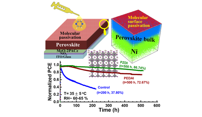
Despite continuous breakthroughs in device efficiency, the stability of HPSCs is still a stumbling block to their competitive reliability in practical applications. To evaluate the device stability, we tracked the device parameters of HPSCs (encapsulated) at the maximum power point tracking (MPPT) conditions under 1 sun irradiation under heat, light, or humidity stress. As shown in (Fig. 6a, b), the device with PZDI treatment demonstrated superior operational device stability under respective monitoring conditions. Interestingly, despite the improvidence in improving device performance, the PEDAI-treated device showed better device stability compared to the control device suggesting the beneficial effect of surface passivation. At elevated temperature (~ 60\(\pm\)5 °C; ~35–40% RH), the performance of the control device dropped to ~ 57.82% of initial PCE in 1000 hours which significantly lowered to ~ 37.80% in 200 hours under heat and moisture stress (T=35\(\pm\)5 °C; RH~ 60–65%). Similarly, HPSCs with PZDI treatment retained ~ 89.48% and 86.74% of original PCE under respective aging conditions. While the PEDAI treated device demonstrated comparatively better device stability than the control device retaining 74.32% and 72.67% of the original PCE under respective aging conditions. These data corroborate that the surface treatment with DIM multifunctional molecules significantly improves the device stability under thermal and humidity stress as a consequence of propitious surface chemistry and interfacial surface modulation with strong adsorption energy.17 This observation indicates that the superior device stability stems from better interface quality and moisture stability in the surface-treated HPSCs.
To consolidate the superior moisture stability data, the water contact angles were taken to study the hydrophobicity of respective HP films (Figure S6c-e). We noticed a significant drop in water contact angle from 66.42° (to~ 0 s) to 42.36° (t ~ 1 min) for the control film. For the PEDAI-treated HP film, it shows a higher contact angle of 84.50° (to~ 0 s) which retains at 78.40° after one minute. Similarly, the PZDI-treated HP film demonstrates a contact angle of 90.60° (to~ 0 s) to 86.20° (t ~ 1 min). It corroborates that the HP films with surface treatment result in excellent moisture tolerance. The moisture resistivity of the passivated film is attributed to its dense distribution on the film surface (Fig. 3h-j), which agrees with the trend of device stability under higher humidity stress.
Moreover, to contemplate the interfacial deterioration under aging conditions, the capacitance-voltage curves of aged devices were measured. A more pronounced C-V hysteresis was seen for the control HPSC (Fig. 6f-h) suggesting a deteriorated interface compared to the HPSCs with surface passivation. This observation substantiates that the control HPSC degrades due to the corrosion of the interfacial junction and increasing dominance of accumulated ions at the interface.47 A sharp transition of the M–S curve in the device with PZDI treatment indicates a smaller depletion layer capacitance (Cdl) that is attributed to low interfacial defect density. It retains a more stable interfacial junction that stems from intact bulk capacitance (Cg). 48,49 One can see a plateau capacitance (Cs) region for V\(>\)VD which is correlated to interfacial charge accumulation and electrode polarization. A suppressed C-V hysteresis in PZDI-treated HPSC signifies the suppression of ionic motion or interfacial charge accumulation induced with scan directions.38,50,51 This result is in line with an earlier report on interfacial degradation analysis.6 Interestingly, the M-S characteristic features for the aged PEDAI device are not as intact as PZDI treated device. These characteristic disparities indicate that alky amine is rather meticulous for surface passivation as supported by theoretical calculations. Thus, this work corroborates that localized electron density in alkyl amine enhances the interfacial adhesion stabilizing the interface and bulk that is benign for device efficiency and operational stability.