Mechanical exfoliation. Mechanical exfoliation is the most straightforward approach to create atomically thin flakes, especially in the early stages of material characterization and semiconductor device fabrication, i.e., device prototyping. The LMs show strong covalent bonding in the two-dimensional plane and a strong interlayer force attributed to the lone pair electrons, which generate a large electron distribution and electronic coupling between adjacent layers52–53. Owing to antiferroelectric coupling between the in-plane polarized few-layers, it is difficult to receive single monolayers from bulk monochalcogenide crystal35, 54. In comparison to transition metal dichalcogenides, monochalcogenides LMs are more difficult to exfoliate, and therefore, studies on exfoliating such materials and those that compare exfoliation difficulties in this family of layered materials remain limited52–54. The thin and thick flakes are obtained by mechanical exfoliation using the Scotch-tape technique (Fig. 2), the physical mechanism of which was described by Gao et al52. The thickness of such flakes decreases with a geometric progress55. All studied materials were synthetic and purchased from HQ graphene and the 2D Semiconductors company.
To study the degradation mechanism in LMs, flakes were exfoliated directly on Si with a SiO2 oxide thickness of 300 nm. The flakes were exfoliated in the glovebox with a nitrogen atmosphere, where O2 and H2O < 1 parts per million (ppm) was ensured. After exfoliation, the flakes are left exposed to the open laboratory air for variable time intervals from the start of exfoliation till the end of the month. For freshly exfoliated flakes, Raman and PL spectra were immediately measured and compared with the air-exposed ones after they were removed from the glovebox.
During the exfoliation of LMs, a strong dependence of the lateral crystal size on the thickness of LMs flakes was noticed: reducing the thickness makes the lateral size smaller55. This is a well-known phenomenon and the typical flake sizes are listed in Table 1. These sizes vary depending on the material and they are slightly larger for group III LMs materials. Using mechanical exfoliation, we obtained the monolayers for GeS, SnS, GaS, GaS0.5Se0.5; however, for GeSe and SnSe, mechanical exfoliation is more difficult. This is in line with a previous study where authors attributed this difficulty to possible antiferroelectric coupling between layers54,56–58. Jiang et al. synthesized single-layer rectangular SnSe flakes by a vapor transport deposition method, followed by a nitrogen etching technique59. This suggests that the difficulties of mechanical exfoliation are not an obstacle to the direct synthesis of LMs with monolayer thickness. To summarize the difficulty of exfoliation, all tested materials were divided into groups based on the hardening of exfoliation (Table 1). In conclusion, we observe the easier exfoliation of sulfur-containing materials where monolayer is obtainable.
Table 1
Difficulty with the mechanical exfoliation of group IV and III LMs. Low hardening – materials hard to exfoliate and receive monolayer; Strong hardening – easy to exfoliate, monolayer is obtainable.
| Material | Layer size (µm) | Lowest thickness (ML) | Hardening of exfoliation |
| | | Low | Medium | Strong |
| GeS | ~ 10 × 5 | ~ 1–2 | | X | |
| GeSe | ~ 25 × 15 | ~ 15–20 | X | | |
| SnS | ~ 10 × 5 | ~ 1–2 | | X | |
| SnSe | ~ 20 × 15 | ~ 30–35 | X | | |
| GaS | ~ 30 × 20 | ~ 1–2 | | | X |
| GaS0.5Se0.5 | ~ 60 × 40 | ~ 1–3 | | | X |
Surface degradation of group IV layered monochalcogenides. GeS and GeSe are layered orthorhombic crystals with band gaps of 1.69 and 1.7 eV, respectively36,60–65. Images of freshly exfoliated GeS flakes are presented in Fig. S1 in the electronic supplementary materials (ESM). Figure 3 shows the Raman spectra for the exfoliated and air-exposed GeS flakes. For the bulk material, three intense peaks corresponding to the B3g, B3g/A1g, and A1g modes are observed (Fig. 3(a)). The positions of these modes are in agreement with those previously reported in Ref65. For thicker flakes, a significant decrease in the intensity of these modes is observed at the beginning (Fig. 3(b)). We observed that the intensity of the Raman peak does not change significantly with increasing oxidation time, indicating that the oxidation of the upper layer is caused by direct contact with the environment. The top oxidized layer can prevent the oxidation of subsequent layers underneath. A decrease in the intensity can also be recognized for monolayer flakes (see Fig. 3(c)); however, the intensity of the Raman peak is very weak right after exfoliation. In addition, the Raman peaks for monolayer GeS disappear during measurements, indicating their low stability under ambient conditions or/and illumination by laser light.
The PL for bulk GeS is visible at 1.68 eV, whereas for few-layer GeS no PL is detected at room temperature at this excitation power (50 µW), see Fig. 4(a). The PL is on the same level when thick flakes (> 200 nm) are exposed to air, as shown in Fig. 4(b). For the thinner flake (thickness = 90 nm), PL decreased monotonically with time. These differences can be explained by the saturation of the thickness of the oxidized layer on the top of GeS.
Since PL comes from the volume of the material, the oxidized layer of the same thickness is more important in thin flakes than in thick ones. Therefore, for thin GeS flakes, the PL decreases with time because it degrades due to oxidation. Thus, the observation of PL from atomic-thick GeS layers remains very challenging. These types of layers require rapid protection immediately after exfoliation or storage in a suitable atmosphere.
For understanding the main differences between the stability of GeS and GeSe materials, we repeated all measurements for the exfoliated GeSe. The bulk GeSe crystal is a semiconductor with an indirect band gap at ~ 1.7 eV36, 60–61, 65–69 and therefore, no PL is observed for the GeSe flakes. The Raman spectra for freshly exfoliated and air-exposed GeSe flakes are shown in Fig. 5. Given the difficulty in carrying out the exfoliation for this material, the thin layers were excluded. For exfoliated thick flakes, the A1g(1), A1g(2), E1g, and E2g modes identified in the Raman spectra are consistent with those reported in Refs.60–61, see Fig. 5(a). The material stability study under laboratory conditions shows a decrease in the intensity of the Raman peaks immediately after exfoliation and further decrease, which saturates (Fig. 5(b)).
The comparison of the degradation effects in GeS and GeSe materials indicates higher oxidation for the GeSe material. The main reason is the presence of Se in GeSe, and the Se protrusions during exposure at ambient conditions. The results from EDS confirm the oxidation process in this material (see Fig. S2 in ESM).
As shown in Fig. 6, the characterization of the oxidized flakes by SEM indicates two types of protrusions. The first type are on the edges of each layer flake (Fig. 6(a)), whereas the other ones are observed on the entire surface of the thick flakes (Fig. 6(b)). A similar type of protrusion is found for the layered HfSe270. In HfSe2, they are related by the growth of Se-rich blisters when Hf oxidizes into HfO2 and eliminates Se at the flake surface. The mechanism is similar during GeSe exfoliation under laboratory conditions. The protrusions at flake step-edges have a higher density because of dangling bonds that appear at these edges after mechanical exfoliation. These dangling bonds can act as the most appropriate nucleation sites for the growth of protrusions70. Such features were not observed for GeS flakes, which means that the observed phenomenon is related to the Se component of the material that is oxidized; thus, in the case of monochalcogenides and dichalcogenides, it is GeSe and HfSe2, respectively.
Detailed observations of flake degradation are established for the GeS and GeSe material using STEM and EELS spectroscopy (Figs. 7–9). The TEM images of the studied flakes are represented in Figs. 8 and 9. The EELS spectra for GeSe are collected from the crystalline (red rectangle in Fig. 7(a)) and amorphous areas (blue rectangle in Fig. 7(a)). Figure 7(b) shows that the oxygen (O-K) content is clearly visible for the amorphous material. The amorphization process of the crystalline phase for both materials is shown in Anim. 1 and Anim. 2 in the ESM. As these measurements are performed under vacuum conditions, the process is attributed to the interaction of the electron beam with the thin layered material. However, some oxidation occurs during the transfer of the sample to the microscope. A very important conclusion from this observation is that the process of flake degradation is anisotropic, i.e., stronger degradation is observed at the edges of the fake. The same can be expected during oxidation in ambient conditions. Ge bounds in GeS and GeSe flakes are saturated on the surface of the flakes while they are more active at flake edges and can be easily saturated by oxygen, leading to stronger flake oxidation from edges. On the flake surface, the oxidation process is promoted by S (Se) vacancies or other defects. The stronger degradation of GeSe flakes can be attributed to the poorer surface quality (higher concentration of Se vacancy), which correlates with the observation of Se protrusions on the surface shown in Fig. 6.
SnS and SnSe are other representatives of group IV LMs. SnS has an indirect band gap of ~ 1.24 eV for bulk and ~ 1.96 eV for the monolayer71–74; however, this is currently being investigated75, and therefore, it is not discussed in this paper. For the bulk SnSe, the band gap is indirect at ~ 1.0 eV for the monolayer and it decreases with an increase in the number of layers76–80.
In the Raman spectra of the SnS samples, five modes are clearly visible (Ag(1), Ag(2), Ag(3), B2g, and B3g), see Fig. 10(a). The positions of SnS modes are previously reported72–74. The intensity of these modes decreases after exfoliation and saturate with time (Inset in Fig. 10(c)). In addition, PL is observed for this material. The maximum PL for a bulk crystal is located at 1.31 eV, and it shifted for the thick flake to 1.28 eV (Fig. 10(c)) and was not observed for the few-layer flake. With an increase of the exposition time under laboratory conditions, PL shifts and widens, as shown in Fig. 10(b) and Fig. 10(d). This effect could be related with the appearance of SnOx on the flake surface; its position is determined as per the method presented by Peercy et al81. However, the origin of this PL peak is still unclear, but this is not discussed in our paper.
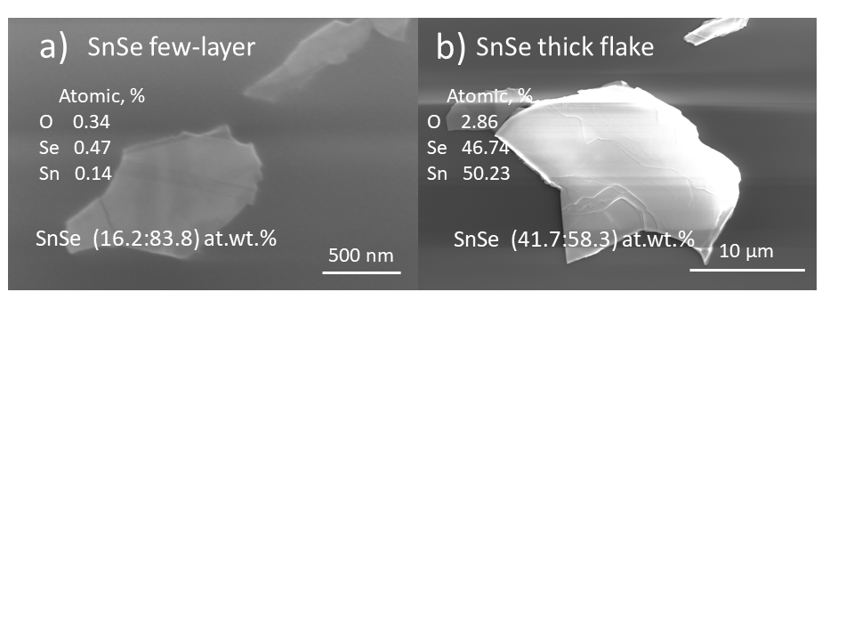
The most important point obtained from studying the PL for this material is that this peak is sensitive to sample exposure to air, which is evidence of sample degradation over time. Figure 10(c) shows the Raman spectra of a thick SnS flake recorded at different time intervals. In this case, a decrease in the intensity of the Raman modes is clearly observed and attributed to sample degradation with time. This effect is considerably stronger for very thin SnS flakes (few layers) because the disappearance of Raman modes is observed during measurements. This observation confirms the immediate degradation of the thin SnS flakes after exfoliation when the sample is exposed to air. In addition, the effect of the oxidation of the SnS and SnSe flakes is clearly confirmed by EDS (see Figs. S3 and S4).
The Raman spectra for the bulk SnSe shows the Ag(2), Ag(3), Ag(4), and B2g(3) modes at positions 71, 112, 133, and 150 cm− 1, respectively (Fig. 11). These modes were previously characterized by Yang et al71. The thick flakes (down to 100 nm) show these peaks; however, for thin flakes down to a few layers, Raman modes appear only at 306 and 438 cm− 1, as shown in Fig. 11(a).
Surface degradation of group III layered monochalcogenides. GaS has an indirect band gap of 2.59 eV at laboratory conditions48, 72–74, and it retains this indirect band gap with thickness reduced up to the single layer48. Therefore, band gap-related emission is difficult to observe for these samples and cannot be used as a marker for material degradation study. In this case, Raman measurements were used to evaluate the degradation process of the GaS flakes. Figure 12 shows the Raman spectra for the GaS exfoliated flakes. The intensity of Raman peaks strongly depends on the thickness of the GaS flake (Fig. 12(a)), which is consistent with the previous studies on this material73–74.
Two modes are visible for bulk and thick flakes: A1g(1) and A1g(2) (Fig. 12). In the case of monolayer, only peak from substrate is visible, see Fig. 12(a). The intensities of GaS modes after a few days of exposure changed slightly. A decrease in the intensity was observed after three weeks, which indicates the considerably high stability of GaS under ambient conditions. This statement is similar with the previously reported by Afaneh et al43. The appearance of oxygen on the surface is confirmed with EDS analysis as shown in Fig. S5.
Unlike GaS, GaSe is less stable in air, and a peak associated with the α-Se phase appears after 2 h of exposure43,48,50–51,56. We investigated the stability of the GaS0.5Se0.5 alloy, which is a mixed crystal of GaS and GaSe58,75–76. The Raman spectrum shows three peaks, which correspond to the A1g(1), A1g(2), and Eg(1) modes, positioned as reported by Gasanly et al75. The thickness-dependent Raman spectra for GaS0.5Se0.5 and the oxidation studies are illustrated in Fig. 13.
After two weeks of exposure in ambient air, a new Raman peak was observed at 232 cm− 1 in the Raman spectrum for few-layer; this corresponds to Ga2O343. The oxidation of GaS0.5Se0.5 under ambient air generates Ga2Se3 and Ga2O3. These oxides were also noticed by Rahaman et al50; they reported that the peak at 433 cm− 1 probably appears because of S-S stretching arising from cluster edge dimers57. The appearance of oxygen after air exposition is confirmed in Fig. 13(b) by the peak at 232 cm–1. For very thin GaS0.5Se0.5 flakes, the intensity of the Raman mods drops significantly after exposition in air; these spectra are not shown in Fig. 13.
A comparison of the stabilities of GaS and GaS0.5Se0.5 under ambient conditions indicates higher resistance to the degradation of the GaS material. This assumption is visible from the comparison of the decrease in the intensity of the Raman modes for both materials. Therefore, the GaS0.5Se0.5 alloy is less resistant; after three weeks of exposure to ambient air, almost all Raman modes are weaker and difficult to detect. The lower resistance of the GaS0.5Se0.5 compound is attributed to the addition of Se atoms. Results from the EDS analysis suggest a stronger oxidation of this material, as shown in Fig. S6.